Designing PCBs: Advanced SMD
SMD is a form factor for a component (as opposed to thru-hole). A pad is what the pins of an SMD component rest on to be soldered. Presumably (I haven't used eagle pcb specifically), SMD is used to add an entire component to the layout, while pad is used for extraneous things, such as heatsinking. The ADD tool also has search functionality -- very helpful when you have to navigate through dozens of libraries to find a part. Andererseits ist die Funktion Mirror im Board-Editor ohnehin nicht sehr nützlich, denn alle Bauteile, die man wenden kann, kann man stattdessen auch einfach drehen. Using EAGLE: Schematic
These are the tutorials and concepts you may want to know before starting this tutorial: How to Read a Schematic. PCB Basics. How to install and setup Eagle PCB software. How to layout PTH PCBs: Schematic. How to layout PTH PCBs: Board Layout. Creating SMD Footprints. They have a pretty good interface for inspecting your gerber files. To add a schematic to a project folder, right-click the folder, hover over "New" and select "Schematic". Designing PCBs: SMD Footprints
Use the following solution: Open the PCB library and the footprint to edit in EAGLE. Create a pad shape on Layer 1 (Top - Copper) using the polygon tool. Create in the same way or copy this shape to Layer 29 (tStop). Repeat step 3 for the Layer 31 (tCream). In the middle of the shapes put a small SMD pad. Save the 2D footprint. Arbitrary Pad Shapes. This'll store the copied group into your operating system's clipboard, and you can use paste to place it somewhere. Click on each pad I started with 16 and worked my way right and adjust the X coordinate. Be sure to give some sort of description to your package. Designing PCBs: SMD Footprints - SparkFun Learn
This tutorial will show you how to create a custom SMD footprint and schematic symbol library. This is a crucial skill for any hacker who wants access to the latest technology via SMD modules or new SMD ICs. SMD ICs are incredibly small. Learning how to make footprints that work with these tiny part is a crucial skill. This is incorrect. Die Entwickler haben aber festgestellt, dass das Spiegeln von Footprints im Board-Editor an sich keinen Sinn macht, weil man die Bauteile ja nicht "kopfüber" bestücken kann. Designing PCBs: SMD Footprints - SparkFun Learn
I was creating a custom power MOSFET package for my project.I found that in EAGLE CAD there are two options - SMD (red symbol) and PAD (green) to specify the physical location of the pins. I could not however find when we have to use SMD and when to. Finally the white line that makes up the board outline should be highlighted. The hard part, sometimes, is identifying which part on a circuit symbol is actually a pin. Connectors are often numbered differently from ICs so read your datasheet closely. Eagle förändring smd3
So I have a design in Eagle with a few SMD components that have pads that should be grounded. I've done a copper pour (draw polygon->name GND->Ratsnest) to create a top ground plane. On some of my components the ground plane connects to the SMD pad, but only by four narrow traces (such as below). This will make all the ground airwires disappear. Move it directly onto the end of the capacitor and click to drop it. We can infer this from dimension E 0.
Eagle förändring smd2
4 I'm doing my own component in Eagle for a PCB design. This is the footprint that the manufacturer gives: But I have a problem with the SMD roundness when I try to draw the SMD footprint at the sides. Be sure to give some sort of description to your package. Du kommst so ca. These signifiers can help the DRC design rule check and ERC electrical rule check to detect potential problems with your board. 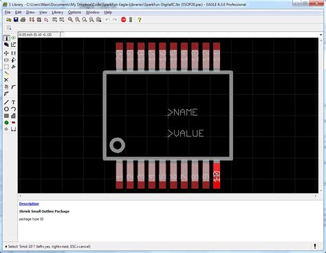
Designing PCBs: Advanced SMD - SparkFun Learn
Leading The Industry in Product Availability, Speed of Service, Responsiveness, and More. Order Antennas, Resonators, Transformers, and More from Abracon at DigiKey!. Be sure to add a description to your part. For this IC, the pitch is 0. Now how many functional pins does the FTX have?